By Patrick Mullen.
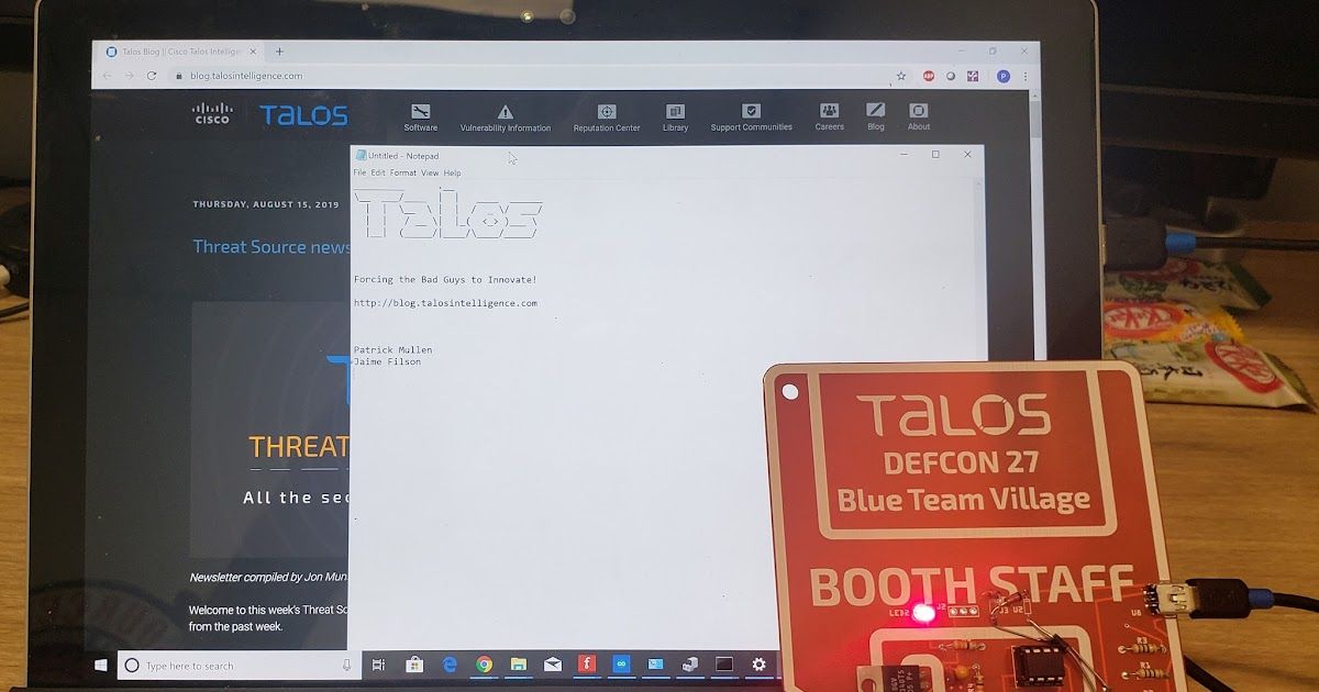
We want to thank everyone who stopped by the Cisco Talos booth at DEFCON's Blue Team Village earlier this month. We handed out these badges at our area where we had Snort rules challenges, reverse-Capture the Flag and recruiters ready to answer attendees' career advice questions.
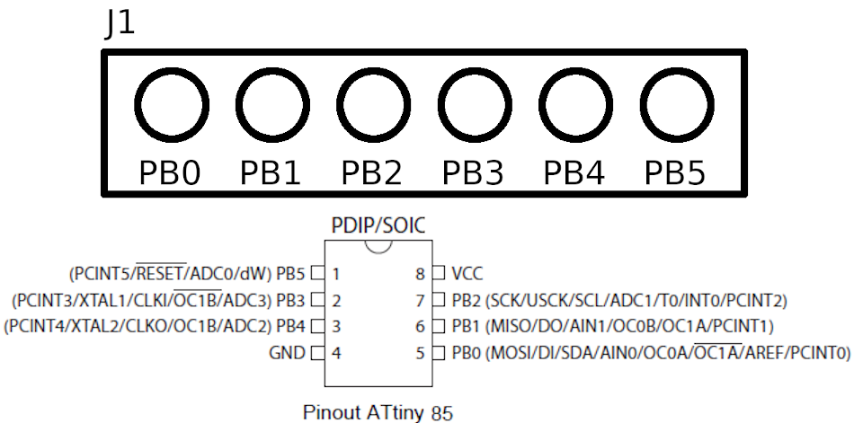
Unfortunately, there were two bugs in the board as created, which should be expected when it was created in such a short time, but we have a guide for how you can fix these. Once these bugs are fixed, you'll have a fully functional Digispark clone that can be used for several projects, including impersonating a USB keyboard, as our example sketch does. You can also attach leads to the open jumpers to get full access to all of the pins from the ATtiny85 to drive your own projects.
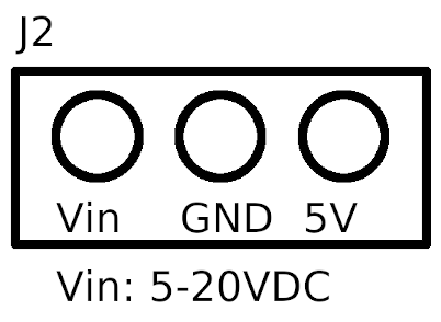
Power is provided directly by the USB port when used as a USB device, by a USB charger, or via J2 at
the top of the board. The center pin is GND, the right pin is for regulated for five volts, or the left pin can handle anywhere from 5V to 20V. During Defcon, we powered it with a nine-volt battery for convenience.
The first bug is really easy — diode D1 on the lower right of the board has the line indicating the direction for the cathode on the wrong end due to using a faulty schematic.
The second bug took a bit more creativity to overcome, but the actual assembly isn’t too difficult and makes the build that much more fun. The issue is that the schematic for the USB port was rotated, so we need to tweak the circuit so everything connects to the right place. I think the end result adds character to the badge and is quite effective.
Tools needed:
- Small straight slot (flat head) screwdriver
- Soldering iron with a small tip
- Solder
- Small wire cutters
- Small needle-nose pliers are helpful
- Multimeter, or at least a continuity tester (beeps when two connections are attached)
- A magnifying glass can be useful to check your work
- Arduino IDE for programming the chip
- ATtiny85 w/ Digispark bootloader. Bootloader is needed for programming over USB
- 8 pin DIP chip holder
- 5V power regulator
- Through-hole mini USB connector
- (2) 3.6V zener diodes
- (1) Schottky diode
- (2) 75 ohm resistors (or 100 ohm or 66.5 ohm as in schematic)
- (1) 1.5k ohm resistor
- (2) 330 ohm resistors
- (2) LEDs
- (1) 0.1 uF capacitor
- (1) 4.7 uF capacitor

Prepare the board
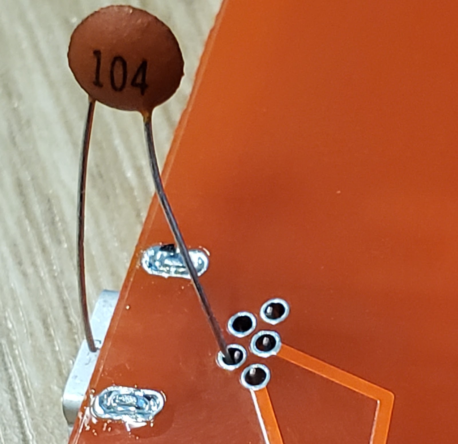
To rewire the USB port in a way that is easier to build the board, we are going to have to cut one of the lines on the board. If you want to be fancy, you can do this by drilling through the board, but scratching through the conductor (“line/wire”) with a straight slot screwdriver is more than sufficient.Be careful to not hit one of the other lines and if you have a continuity tester (or a multimeter set on resistance and verify infinite resistance aka open connection), it’s always good to verify you’ve done so successfully and completely.
The
line we want to cut (viewed from the back of the board) starts from the bottom-most connector of the USB jack, but cut it *after* the connection hole, before the ‘T’ junction. See the photo since I’m not getting paid by the word and don’t want to write a thousand of them. Note the multimeter is demonstrating there is no connection between the pin on the USB connector and that connection point on the board after our “cut.”

Prepare the USB connector
Thankfully, one of the USB connections is not used and this allows us to modify the jack to get rid of the unused pin and then create a bridge on the board to bring the pin that is used over to the circuit where it was originally supposed to be connected.To remove the unused pin, flip the USB connector over so the pins are on top and the “open-end” is to the left. The pin you want to remove is the top left one.
I had great success by using the small straight slot screwdriver to bend the pin toward the “back” of the connector (to the right in the photo), then using needle-nose pliers to wiggle it back and forth until it broke off cleanly.

Solder on the USB connector
NOTE: We are going to need to bridge a connector here and to keep everything you need within the kit, we’re going to use part of a lead from one of the components.- Put the USB connector into the holes from the front side of the board and flip the board over. You can use the power regulator (the black component with the metal fin) to keep the board level while you solder.
- Solder the two positioning holes on the left to keep the connector from moving while soldering the pins.
- Put one of the legs of the burnt orange / brown capacitor into the hole on the left with the pin sticking through it. Again, a picture helps here. All we are doing here is using a bit of that nice, thin wire from the capacitor to bridge between the two connectors on the left.
- Solder all FOUR of the pins from the USB connector. DO NOT SOLDER THE EMPTY HOLE. These pins and these holes are really small. Now would be a good time to clean your soldering tip and make sure you don’t use too much solder and bridge connections.
- Cut the leg that you soldered into the hole about halfway up the leg. You don’t need much of the leg to go through the board when you solder the capacitor into the circuit, and you only need enough to reach to the open connection on the USB port.
- Bend the cut leg over to the open connector, lay it across the connector being careful not to short any others, and solder it in place. Using your screwdriver can provide extra leverage and precision to bend the bridge all the way to the board.

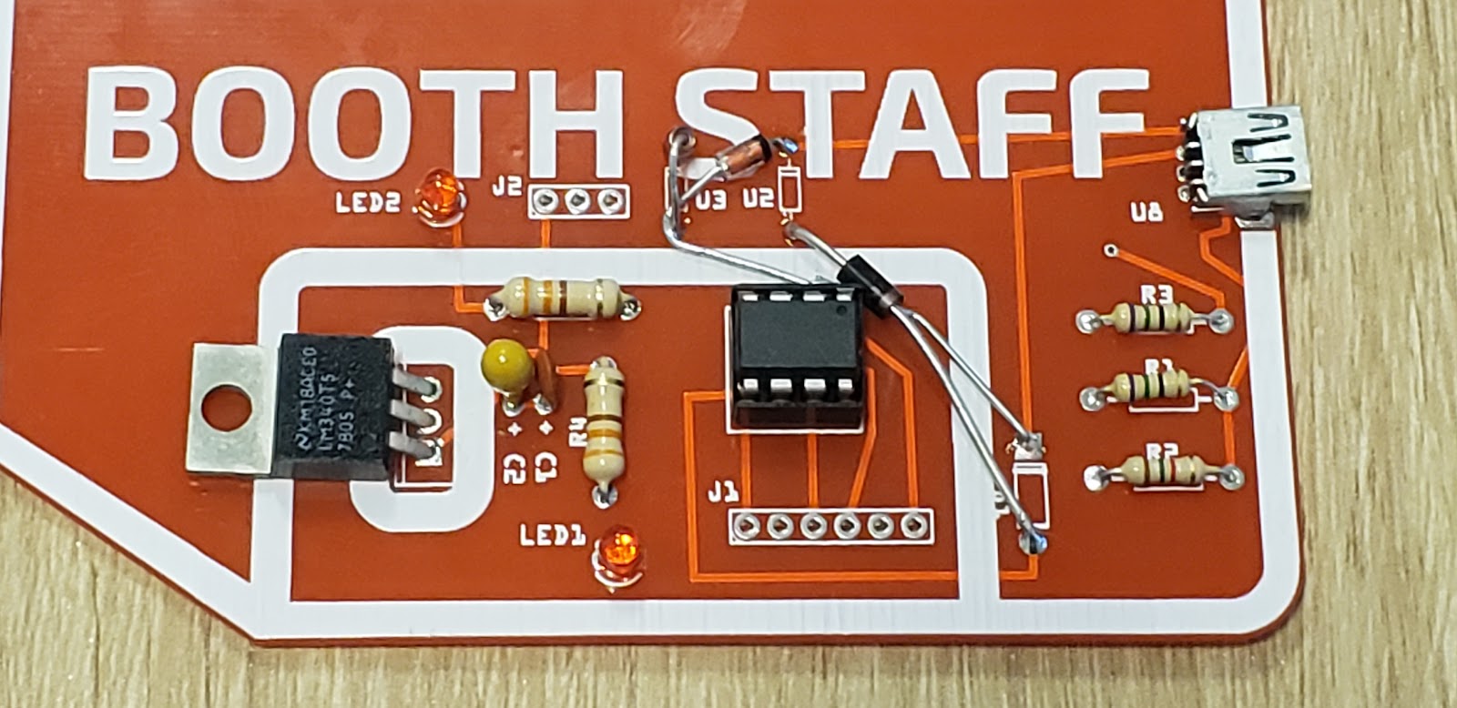
Soldering on the "normal parts"
You can now solder on all components except the three diodes. The diodes are the “glass-looking” red things with the black line and the black with silver line component.
Notes for assembly — be aware that some parts are unidirectional.
- The LEDs are unidirectional. The long leg goes through the hole with the square contact around it. NOTE: The two LEDs have square contact on opposite sides.
- The yellow capacitor is unidirectional. The long leg goes toward the "+" toward the bottom of the board. The burnt orange/brown capacitor can go in either way. The capacitors are connected in parallel, so it doesn’t matter which goes into the C1 or C2 connection.
- R4 and R5, near the power regulator, are 330 ohms. In the kit, they are the fat resistors with orange-orange-brown stripes. Note the gold stripe on the resistors refer to the tolerance/"quality" of the resistor and doesn't really matter for this circuit.
- R3 and R1, the top two resistors below the USB connector, are 75 ohms, with purple-green-black stripes. If your kit does not include these resistors (we bought every 75 ohm resistor at Fry's in Las Vegas), 100 ohms is a common size that will also work.
- R2, the bottom resistor on the right side, is 1.5k ohms and has brown-green-red stripes.
- The big blue resistors in the kits are not used. They were supposed to be 66.5 ohms. They are 66.5 *thousand* ohms. Oops.
- The chip connector has a notch on it that lines up with the break in the silkscreen to the right. This is used to indicate pin 1 on the chip. Do not have the chip in the socket while soldering it in place. Do not forget to trim the ends of the leads off after soldering.
- The power regulator (the black thing with the metal fin) has a line on the board on the left side that indicates where the cooling fin goes. When connecting this component, I find that leaning it to the right when soldering it on will give you a little extra room to bend it over to the left so it’ll lie flat when finished.

Soldering on "funky bits"
Now, we need to reverse the 5V and GND circuits. I think steps 1 and 2 below make more sense if you see what the circuit will look like before reading it, so this is what you should have after step 2:
- Take one of the zener diodes (the little glass-looking things with the red underneath and the black stripe). The black stripe lines up with the stripe on the circuit board printing. But, because this is the “funky” section, we’re going to connect it “weird.”
- Insert the zener diode into the *left* diode slot, U3, but stick it in so it points straight up, with the black line down against the board.
- Solder it in the straight-up position.
- When you cut the lead on the back of the board, SAVE THE CLIPPING. We’ll need it in a moment.
- Leave the diode in this position for now.
- Take the other zener diode, and bend the end with the black stripe as if you were going to mount it normally, but leave the other leg straight.
- Insert it into the top connector of U2 (so the stripes match) but angle it to the left so it crosses the U3 silk screening before you solder it on.
- You may find that with the other components on the board, and the relative sizes of the wire and the hole, that it’s easier to solder this component from the top if you leave yourself room after the bend. Cut off the extra in the back of the board and solder from the back for a good connection if necessary.
- Bend the loose leg of U2 so it goes around the bottom hole of U3 and across the top of the chip holder. This is easier with needle-nose pliers. We will be soldering this leg to the bottom leg of U3, so don’t worry about keeping a distance from the wire.
Connect the zener diodes together
- Returning to U3 (the zener diode on the left), bend the remaining wire forward, through the bottom hole for the diode, and solder it into place. Using needle-nose pliers to make the bend and insertion may make it easier. Be gentle so you don’t snap the diode in half. There’s no reason to get this too tight and risk breaking the component.
- Solder the bottom leg of U2 to the bent leg of U3. Don’t forget to make sure that U3 is soldered into the board as described in the previous step.
- Connect the zener diodes to GND
- Solder the leg you removed from U3 into the top connector for D1, with the leg sticking straight up out of the board. We are going to bend it so we can connect it to the tail of U2 (which has been bent around the bottom wire from U3).
- Bend the leg up to meet the long lower leg from U2 and solder them together. You should now have a connection from the top of D1 to both diodes, at the bottom of U3.
- Solder the schottky (black w/ silver stripe) diode

- For this one, the silkscreen is backward because the schematic I was using had this diode backward, so ignore the marking on the board. We are using the long legs of this diode to make a long connection to fix the circuit without needing additional wire. With the fix, the proper connection is for the end with the silver stripe to connect to the bottom of D1 and the other end to connect to the bottom of U2. Feel free to tuck this in as much as you can, but make sure you are clear of any wires touching. If you’re feeling particularly frisky, you can use the diode itself as an insulator against the connector for U2 that goes around the chip carrier, or some electrical tape.
- Insert the chip
- There is a little dot on top that indicates pin 1. That goes toward the end of the chip carrier with the indent (to the right of the board).

Programming the board
I'm going to outsource the programming of the board now to this YouTube tutorial. Remember, this board uses the ATtiny85 chip and is a Digispark clone. If you have any issues, search for those names online and you should get what you need.Everywhere the creator of this video says “Digispark board,” hear “Talos Defcon 27 Blue Team Village badge” because they are the same.
- Open the Arduino IDE and load the Digispark board managers (1:48 in the video).
- Load the drivers (3:54 in the video). Hopefully, with our board and the bootloader we have installed, this step will be easier for you. He provides information and links if you have troubles.
- Load the Arduino IDE (7:24 in the video). If you want to do the blink sketch he talks about, you’re welcome to do so. Or just go right to the excitement and do the next step instead!
- Copy and paste this sketch
Now you can upload the program. Don’t forget to unplug the badge (if necessary) and plug it in when the IDE tells you to (as described at 9:07 in the video).
Now that your badge is programmed, you no longer need the Arduino IDE or drivers to control other computers. Just plug it in, wait five seconds while the board initially identifies itself as an Arduino then disconnects and reconnects as a keyboard, and watch it do its thing. LED1 is a status light as programmed in the sketch — it turns on when it starts typing and turns off when it’s completed all of its commands.
If you want your badge to send different commands, change the lines that call the function type() and tell it to type something else. Please note that these chips have extremely tiny memories and unfortunately the DigiSpark library takes up a lot of room so you don’t have a ton of text you can type, but you do have a fair amount. If you look into trimming the installed size of the code you should be able to get more program onto the chip.
Some other notes on the badge:
- If you get female lead connectors and solder them to J1 and J2, you can use the ATtiny85 to do whatever you want, as long as you only need a few data lines and a small memory. You can, of course, solder to the leads directly if you want, but by putting in female leads you can make a reusable circuit. Note it is probably not a good idea to drive the data pins however you want while connected to a USB data cord.
- J2 is for external power, so you can run the board while not connected to USB. The middle connector is ground. The connector on the right is for 5V *only*. The connector on the left can run 5V-20V DC.
- You can also power the circuit using a USB charging cable, but as stated above, it’s not recommended to be connected to the computer USB data port if you’re running a sketch that is not specifically for driving USB data, like a keyboard.
- You can program it either through the USB as you did above or by using something like an Arduino UNO as an ISP as described in this video.
- If you want to change the bootloader (or if you get a stock ATtiny85 that doesn’t have the boot loader we installed on the ones in the kit), directions are in this video.
We hope to continue and do other badges in the future, hopefully, next time without bugs! We hope everyone had a great time at Hacker Summer Camp and look forward to next year where we'll have all new challenges, badges and other fun things to poke at.